Nanobubbles in Microelectronics: Precision Cleaning
Unveiling the Power of 30nm Nanobubbles
In the realm of microelectronics, where precision is paramount and cleanliness is king, the advent of nanobubble technology has emerged as a game-changer. Our cutting-edge nanobubble machine takes center stage, producing 30nm bubbles that redefine the standards of precision cleaning in the microelectronics industry.
The Precision Revolution
In an era where every nanometer counts, the significance of utilizing 30nm nanobubbles cannot be overstated. These ultra-small bubbles exhibit unparalleled efficacy in removing contaminants at the microscopic level, ensuring a level of cleanliness that was once deemed unattainable.
The Science Behind 30nm Nanobubbles
Our nanobubble technology operates on the principle of ultrasonic cavitation, creating bubbles with a diameter of precisely 30nm. This optimal size allows the bubbles to penetrate even the tiniest crevices on electronic components, dislodging and lifting away particles with remarkable efficiency.
Superior Cleaning for Microelectronics
Traditional cleaning methods fall short when it comes to addressing the minute intricacies of microelectronics. Our 30nm nanobubbles, on the other hand, provide a superior cleaning solution, leaving no room for contaminants to compromise the functionality and longevity of delicate electronic devices.
Advantages of Our Nanobubble Machine
1. Unmatched Precision
The key differentiator lies in the precision of our nanobubble machine. By generating bubbles at the 30nm scale, we ensure that no particle, regardless of its size or location, goes unnoticed. This level of precision sets our technology apart in the competitive landscape.
2. Gentle Yet Powerful
While the cleaning power of our nanobubbles is extraordinary, their gentle nature ensures that delicate electronic components remain unharmed. This delicate balance between power and finesse makes our technology the ideal choice for microelectronics applications.
3. Eco-Friendly Solution
In an era where environmental sustainability is a non-negotiable factor, our nanobubble machine takes the lead as an eco-friendly cleaning solution. The process is devoid of harsh chemicals, minimizing the ecological footprint and aligning with global sustainability goals.
Applications in Microelectronics
1. Semiconductor Manufacturing
In semiconductor manufacturing, the cleanliness of wafers is paramount to ensure the functionality of integrated circuits. nanobubble technology excels in this domain, offering a level of cleanliness that surpasses conventional cleaning methods.
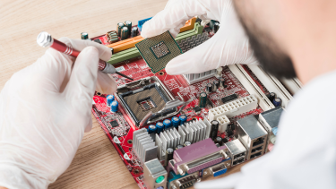
2. Printed Circuit Board (PCB) Assembly
Precision is the soul of PCB assembly, and the nanobubble machine ensures that every nook and cranny of circuit boards is free from contaminants. This, in turn, enhances the reliability and performance of electronic devices.
3. Optoelectronics
Optoelectronic devices, such as sensors and LEDs, demand a pristine environment for optimal performance. 30nm nanobubbles guarantee a level of cleanliness that enhances functionality and extends the lifespan of these critical components.
Outranking the Competition
In the realm of microelectronics, information is key. As the pioneers of 30nm nanobubble technology, we stand out in a sea of competitors. Our commitment to precision, innovation, and environmental responsibility positions us as the preferred choice for industries seeking superior cleaning solutions.